Xilinx Verilog Tutorial
CSE 372 (Spring 2005): Digital Systems Organization and Design Lab
The programmable logic boards used for CSE 372 are Xilinx Virtex-II Pro development systems. The centerpiece of the board is a Virtex-II Pro XC2VP30 FPGA (field-progammable gate array), which can be programmed via a USB cable or compact flash card. The board also features PS/2, serial, Ethernet, stereo audio and XSGA video ports, user buttons, switches and LEDS, and expansion ports for connecting to other boards.
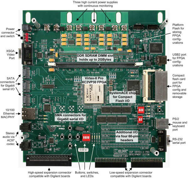
The Xilinx Virtex-II Pro Development System.
To see some of the features in action, you can run the board's built-in self test.
Caution!
The boards contain many exposed components that are sensitive to static electricity. Before touching the boards, try to remember to discharge any static electricity you may have built up by touching a grounded piece of metal (i.e. part of the desk). Especially remember to do this after you have been walking around the room on the carpeted floor (please keep your shoes on).
Built-in Self Test
First, set up your board by plugging the power cable into the connector on the upper-left corner of the board. Connect one of the monitors at your workstation to the display port on the left side and connect a keyboard to one of the PS/2 ports on the right side. If you have headphones, you can connect them to the amp out or line out ports on the left side of the board to hear tones, but do not put them on your ears, as the volume will be loud. Finally, you must set the configuration switches to load the self-test. Locate the blue component on the right side of the board with two white switches on it (SW9). Set both of the switches to on/up; this will load the "golden" self-test configuration from the PROM.
Turn the power switch (next to the power cable connector) to on. LEDs will turn on and flash, and the self-test should appear on the monitor. The red "System ACE error" LED will blink because no compact flash card is inserted into the board; this is normal. If you type on the keyboard, the last keystroke will be displayed on the monitor. The user switches (the blue component with four white switches, SW7) can be used to turn the user LEDs (D7-10) on and off. Pressing the five pushbuttons will emit tones from the audio output ports. Finally, notice the reset button on the right side of the board (next to the PS/2 ports); if you hold this button down for two seconds, the board will reset and reload the self-test.
I. Preliminaries
Before beginning the tutorial, it is recommended that you map your personal Eniac account to a drive on your Klab computer by following these instructions: Mapping Eniac in Ketterer Lab.
Warning
Do not save files to the local machine. These machines are not backed up and are unprotected, so others can see your files.
Warning
Make sure you disconnect your network drive when you are done working in the lab. The easiest way to do this is to restart the computer when you leave.
The software for programming the FPGA is the Xilinx ISE Project Navigator. In the KLab, open the software from the desktop icon Xilinx ISE 7.1i or from Start -> Programs -> Xilinx ISE 7.1i -> Project Navigator.
II. Creating a new project in ISE
An ISE project contains all the files needed to design a piece of hardware and download it to the FPGA. Go to File -> New Project to create a new ISE project. Give the project a location on your Eniac drive and enter a name for the project, such as "tutorial". Set the Top-Level Module Type to HDL and click Next.
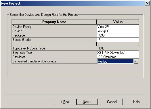
The following screen allows you to set the properties for the FPGA you will be downloading your design to. For our boards, the correct settings are Device Family = "Virtex2P", Device = "xc2vp30", Package = "ff896", and Speed Grade = "-7". Set the Synthesis Tool to "XST (VHDL/Verilog)", Simulator to "ISE Simulator", and Generated Simulation Language to "Verilog" and click Next.
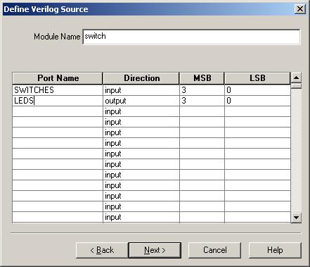
On the next screen, click the New Source button. Select Verilog Module from the list and give the module the file name "switch". A Verilog module is a self-contained hardware unit with an interface of inputs and outputs, which are specified on the next screen.
This screen takes your inputs and outputs and automatically generates the code for your module.
Note
You can have multiple modules per .v file, and you do not have to use this wizard to add a module.
Define two ports: "SWITCHES", an input with a MSB of 3 and a LSB of 0, and "LEDS", an output with a MSB of 3 and a LSB of 0. MSB and LSB stand for most-significant bit and least-significant bit, so these two ports are vectors with four bits/wires.
Click Next and click Finish on the next screen. This will bring you back to the New Project window; click Next twice and Finish once to generate your module.
III. Coding your switch module
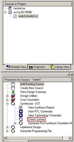
Once your module is generated, the main ISE Project Navigator view appears. There are four main windows in the Project Navigator: Sources in Project, Processes for Source, console output, and the editor. The Design Summary tab on the editor window will be selected after you generate your new module; for now, you can close this tab with the X button in the upper-right corner.
Select the switch.v tab in the editor window. If this tab ever gets closed, you can open the file again by double-clicking on it in the Sources in Project window. The switch module will link the four user input switches on the board to the four LEDs next to the switches, so toggling the switches will turn the LEDs on and off. The values of the switches are inputs to the module, and the signals to the LEDs are outputs from the module. To connect the switches to the signals, just add one line of Verilog code to the module:
assign LEDS[3:0] = SWITCHES[3:0];
Save your file after entering the code. When you are finished, your module should look like this:
module switch(SWITCHES, LEDS);
    input  [3:0] SWITCHES;
    output [3:0] LEDS;

    assign LEDS[3:0] = SWITCHES[3:0];

endmodule
To compile your Verilog code, make sure the switch.v file is highlighted in the Sources in Project window, expand the Synthesize item in the Processes for Source window and double-click Check Syntax.
The console should not display any errors under the HDL Compilation section, and a
 should appear next to Check Syntax. If you get compilation errors, resolve them (ask a TA for help if necessary) before continuing.
IV. Assigning ports to pins
For the ports in the module (SWITCHES and LEDS) to control the components on the board, they must be connected to pins on the FPGA. To do this, click on switch.v in the Sources in Project window, expand the User Constraints item in Processes for Source and double-click on Assign Package Pins. When prompted to add a UCF file to your project, click Yes.
Xilinx PACE will open up. On the left, the ports of your module will be listed, and on the right is a diagram of the FPGA. Click the Package View tab at the bottom of this window to see a diagram of the unconnected pins on the FPGA.
Each component on the board is connected to a pin on the FPGA. The FPGA pins for the user switches and LEDs are shown in the table below.
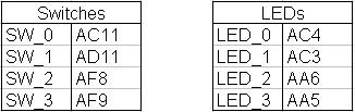
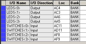
Connect these pins to your module's ports by clicking in the Loc box next to each port and typing in the proper pin. You should see each pin location fill in with blue on the pin diagram. The other information (I/O Std., Drive Str., etc.) does not have to be filled in. Your list of ports should look like this when you are done.
When you are done entering the pin information, click Save. You may be prompted to choose a Bus Delimiter; choose the top option, XST Default: < >, and click OK. You can then close PACE.
Go back to the ISE Project Navigator. You will see a new file, switch.ucf, has been added to the project. By clicking on the filename, then double-clicking on Edit Constraints (Text) in the Processes for Source window below, you can see the format of the UCF file. If you made a mistake in your pin locations or want to change them in the future, you can directly edit the UCF file instead of using PACE.
V. Generating a programming file
Click on switch.v in Sources for Project. In the Processes for Source window, scroll down and double-click on Generate Programming File. This will run all of the processes necessary to create a file that can be downloaded onto the board to program the FPGA. Running these processes may take several minutes; progress is indicated by the bar in the lower-right of the window, the spinning
 icon and output to the console.
When a process completes, a
appears next to it. If any errors occurred during the process, a  will appear next to it. All errors must be resolved before a programming file can be generated. Errors are output to the console, and can be more easily seen by clicking on the Errors tab. Warnings cause a
  to appear next to the process and can be seen under the Warnings tab.
Note
Warnings are usually a sign that something more serious is wrong. It is strongly suggested that you do not ignore warnings and resolve them before generating a programming file.
All processes have run successfully when a
appears next to Generate Programming File. You can scroll up in the Processes for Source window and double-click on View Design Summary to see a report of your design and links to more detailed reports.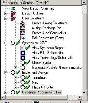
A successful programming file generation.
VI. Programming the FPGA with iMPACT
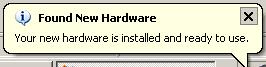
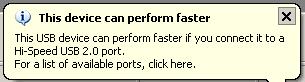
Plug one end of the power cable into a socket and the other end into your board in the upper-left corner. Plug one end of the USB cable into a port on your computer and plug the other end into the connector on the right side of your board. Set the config source switch (switch 1 on component SW9, next to the PS/2 ports) to JTAG (down/off); the settings for the other configuration switches do not matter. Turn on the power switch, located next to the power cable connection, and the green JTAG configuration LED (D20) should turn on. If the board has not been connected to the USB port before, the Found New Hardware Wizard will appear. On the first screen, when asked to connect to Windows Update, select No and click Next. On the second screen, choose to install the software automatically and click Next. Windows will find and install a driver; click Finish on the next screen. You will have to repeat these steps two more times, until Windows installs all of the required software. Installation is finished when you see the following prompt.
If your board has previously been connected to the USB port, or whenever you restart/reset your board, a window should pop up notifying you that Windows recognizes the attached device.
You should see this notification window when you turn on/reset your board.
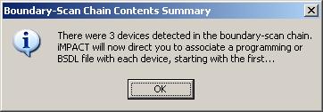
In the ISE Project Navigator, expand the Generate Programming File item in Processes for Source and double-click on Configure Device (iMPACT). iMPACT should open and present the "Configure Devices" window. Select Boundary-Scan Mode and click Next, then select Automatically connect... and click Finish. If iMPACT successfully finds your board, 3 devices will appear in the upper half of the iMPACT window and a dialog box will appear:
If iMPACT fails to find your board, you will see this dialog:
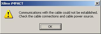
If this happens, click OK, then click Cancel and OK on the next two dialogs. Try again to get Windows to recognize your board by unplugging the USB cable from your board, plugging it back in, then holding down the board's reset button for two seconds. If you cannot get Windows to connect to the board, see a TA. Once you have a connection, click on the Initialize Chain (
 ) button on iMPACT's toolbar to scan for your board again.
When iMPACT successfully scans your board, it finds three programmable devices. The first, "xcf32p", is the board's non-volatile PROM. The second, "xccace", is the System ACE controller (for compact flash). The third, "xc2vp30", is the actual FPGA. You should not ever need to program the first or second devices; do not assign programming files to them or erase them. You will only need to program the third device, the FPGA.
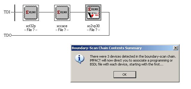
Click OK on the Boundary-Scan Chain Contents Summary dialog and you should be prompted to assign configuration files to the three devices. Skip the first two by clicking Bypass or Cancel. The third device, the FPGA, is programmed with a .bit file. iMPACT should automatically show your project directory and a file, switch.bit. Select this file and click Open, then click OK on the next dialog box to assign the configuration file to the FPGA. Ignore any "clock change" warnings that you may receive.
Note
Sometimes, iMPACT may not prompt you to assign configuration files to the three devices. If it does not, you can do it yourself by right-clicking on the FPGA (xc2vp30) and choosing Assign New Configuration File.
In the iMPACT main window, right-click on the FPGA (xc2vp30) and select Program. Leave all of the boxes unchecked and click OK. The Executing Command box should appear, followed by a blue "Programming Succeeded" message. The red Done LED on the board (D4) should light up, indicating that the FPGA has been programmed. Toggle the user switches, and the corresponding user LEDs should turn on and off. Close iMPACT and choose No when prompted to save your changes.
If your design does not work as expected, close iMPACT, go back to the ISE Project Navigator and make changes. Reset the board by holding down the reset button (you do not have to turn the power off), then generate the programming file again. Double-click on Configure Device (iMPACT) and program the board again.
Note
It is recommended that you follow this order of turning on/resetting the board before starting iMPACT, and it is also recommended that you close iMPACT and restart it before reprogramming your board. Other ways may work, but may sometimes produce unusual behavior. If you see any strange errors in iMPACT, close it, reset your board/connection and try again.
Helpful hints
Hint
The user switches are "active-low", meaning they send a 0 to the FPGA when they are on/up and a 1 when they are off/down. The user LEDs act similarly: they are lit when sent a 0 and off when sent a 1. If you want to experiment and modify your design, keep this in mind. In future assignments, you may be given a controller in which the behavior is reversed to be more intuitive.
Hint
Save your work often. You can also use the "snapshots" feature of ISE to make a backup of your project at any time. In the ISE Project Navigator, go to Project -> Take Snapshot, give it a name and a comment (i.e. the date/time) and ISE will save a snapshot to a subdirectory of your project folder. Snapshots can be managed by clicking the Snapshot tab in the Sources in Project window.
For documentation and links to online help, see the folder C:\Xilinx\372Docs. The links below may also be useful.