Homework 2 - CIS501 Fall 2011
| Instructor: | Prof. Milo Martin |
|---|---|
| Due: | Thursday, October 13th (at the start of class) |
| Instructions: | This is an individual work assignment. Sharing of answers or code is strictly prohibited. For the short answer questions, Show your work to document how you came up with your answers. |
| Note: | This assignment has two parts (see below) due on the same day. Please print out your answers for each part and turn them in as two distinct stapled documents. |
Part A
Pipelining and Load Latency. In the five-stage pipeline discussed in class, loads have one cycle of additional latency in the worst case. However, if the following instruction is independent of the load, the subsequent instruction can fill the slot, eliminating the penalty. Using the trace format used in the first assignment (see Trace Format document), this questions asks you to simulate different load latencies and plot the impact on CPI.
Simulation description. Instead of simulating a specific pipeline in great detail, we are going to simulate an approximate model of a pipeline, but with enough detail to capture the essence of the pipeline. For starters, we are going to assume: full bypassing (no stalls for single-cycle operations), perfect branch prediction (no penalty for branches), no structural hazards for writeback register ports, and only loads will have latency of greater than one. Thus, the only stall in the pipeline is load-use stalls of dependent instructions. As loads never set the flags (condition codes), you can also ignore those.
Scoreboard. There are several ways to simulate such a pipeline. One way is to model the pipeline using a "scoreboard". The idea is that every register has an integer associated with it (say, an array of integers). This value represents how many cycles until that value is "ready" to be read by a subsequent instruction. Every cycles of execution decrement these register values, and when a register reaches zero, it is "ready".
When is an instruction ready? If any of an instruction's source (input) registers are not ready (a value greater than zero indicates it isn't ready), that instruction must stall. In addition, we want to avoid out-of-order register file writes. Thus the "ready cycle" of the destination (output) register must be less than the latency of the instruction. That is, this instruction will write the register after any preceding instructions updated that register.
Executing an instruction If an instruction is ready and writes a destination register, it sets its entry in the scoreboard of its destination register (if any) to the latency of the instruction.
Valid register values. Recall that any register specified as "-1" means that it isn't a valid source or destination register. So, if the register source or destination is -1, you should ignore it (the input is "ready" and the output register doesn't update the scoreboard). You may assume the register specifiers in the trace format are 50 or less.
Algorithm. The below simulation algorithm captures the basic idea. Notice that if an instruction can not execute, nothing happens that cycle. Thus, no new instruction is fetched the next cycle. However, all of the ready counts are still decremented. Thus, after enough cycles have past, the instruction will eventually become ready:
next_instruction = true
while (true):
  if (next_instruction):
    read next micro-op from trace
    next_instruction = false

  if instruction is "ready" based on scoreboard entries for valid register inputs:
    if the instruction writes a register:
      "execute" the instruction by recording when its register will be ready
    next_instruction = true

  advance by one cycle by decrementing non-zero entries in the scoreboard
  increment total cycles counter
Debug trace. To help you debug your code, we've provided some annotated output traces of the first two hundred lines of the trace file (sjeng-1k-2-cycle.txt and sjeng-1k-9-cycle.txt). The format for the output is:
0     1 -1 (Ready)    -1 (Ready)     -> 13  -  -------------1------------------------------------
1     2 -1 (Ready)    -1 (Ready)     -> 13  -  -------------1------------------------------------
2     3 -1 (Ready)     5 (Ready)     -> 45  L  ---------------------------------------------2----
3     4 45 (NotReady)  3 (Ready)     -> 44  -  ---------------------------------------------1----
4     4 45 (Ready)     3 (Ready)     -> 44  -  --------------------------------------------1-----
5     5 -1 (Ready)     5 (Ready)     ->  3  L  ---2----------------------------------------------
6     6 -1 (Ready)    -1 (Ready)     ->  0  -  1--1----------------------------------------------
7     7 -1 (Ready)    -1 (Ready)     ->  0  -  1-------------------------------------------------
8     8 -1 (Ready)    -1 (Ready)     -> 12  -  ------------1-------------------------------------
The columns (left to right) are: cycle count, micro-op count, source register one (ready or not ready), source register two (ready or not ready), the destination register, load/store, and the current contents of the scoreboard (the cycles until ready for that register or "-" if zero).
As can be seen above, the first load causes a stall as it is followed by a dependent instruction (notice that the instruction is repeated, as it stalled the first time). However, the second load is followed by an independent instruction, so no stall occurs.
Answer the following questions:
Before running the simulator, first do a by-hand rough calculation of the impacts on CPI of load-to-use stalls. Use the frequency of loads for the trace you calculated in the first assignment to calculate the CPI (cycles per micro-instruction) assuming a simple non-pipelined model in which all non-load instructions take one cycle and loads take n cycles. What is the CPI if loads are two cycles (one cycle load-use penalty)? What about three cycles (two cycle load-use penalty)?
Based on the above simple calculation, plot the CPI (y-axis) as the load latency (x-axis) varies from one to 15 cycles (the line should be a straight line).
Using the simulation described above, add a second line to the graph described above, but use the CPI calculated by the simulations.
When the load latency is two cycles, what is the performance benefit of allowing independent instructions to execute versus not? (Express your answer as a percent speedup.) What about with three cycles?
Modify your simulator to not model stalling due to enforcement of register write order. How significant is this change's impact on reported performance? Based on this finding, why do processors add hardware to enforce register write order?
What to turn in: Turn in the graph (properly labeled), the answers to the questions above, and a printout of your code.
Part B
Cost and Yield. We talked about cost and yield issues only briefly in class, so this question will introduce you to the cost issues in manufacturing a design.
Your company's fabrication facility manufactures wafers at a cost of $25,000 per wafer. The wafers are 300mm in diameter (approximately 12 inches). This facility's average defect rate when producing these wafers is 1 defect per 250 mm2 (0.004 defects per mm2).
The first step is to calculate the yield, the percentage of chips manufactured that are free of manufacturing defects using the following yield equation (from the appendix of the Patterson and Hennessy textbook):
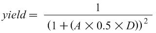
Where A is the area of the chip in mm2, D is the defects per mm2, and yield is a number between 0 and 1. Intuitively, this equation shows that if either the area of the chip or the defect rate increases, the yield decreases.
Based on this yield equation, what is this facility's yield for chips of 100 mm2, 200 mm2, 400 mm2?
Based on the above formula, plot the yield (y-axis) vs the die area of the chip (x-axis). The x-axis should range from zero to 500 mm2; the y-axis should range from 0% to 100%. Plot at least enough plots (say, a few dozen) to generate a smooth curve.
Approximately how many good (defect-free) chips can be made from each wafer for chips of 100 mm2, 200 mm2, 400 mm2? (Ignore the "square-peg-in-round-hole" effect.)
What is the die manufacturing cost for each of these three chip sizes?
Based on the above calculations, on a new graph plot the per-die cost (y-axis) vs the die area of the chip (x-axis). The x-axis should range from zero to 500 mm2; the y-axis should start at zero. Plot at least enough plots (say, a few dozen) to generate a smooth curve.
Assuming 5 million transistors per 1 mm2, on a new graph plot the dollars per billion transistors (y-axis) versus the number of transistors (in billions) on the x-axis.
The above calculation does not include the per-chip cost testing and packaging. Assuming a $50 per chip (independent of the size of the chip) additional cost, add another line to the above graph of the cost per billion transistors with these costs included.
At what transistor count is the cost per transistor the lowest? What is the lowest cost (per billion transistors)?
To investigate the impact of advancing process generations, now consider a manufacturing process that gives 10 million transistors per 1 mm2, but assume all the other costs and defect rates are the same. Add a third curve to the graph to reflect the new cost-per-transistor of this new generation of manufacturing.
With this new data, at what transistor count is the cost per transistor the lowest? What is the lowest cost (per billion transistors)?
Although you've calculated the design point with the lowest cost per transistor, why might a company choose to sell a chip with a number of transistors that is smaller or larger than this minimum per-transistor cost point?
What to turn in: Turn the answers to the above questions and three graphs (properly labeled): (1) yield, (2) cost per die, (3) cost-per transistor (with has three curves).
Addendum
- None, yet