Lab 3 - LC4 Pipelined Processor With Instruction Cache
CIS 371 (Spring 2013): Computer Organization and Design
| Instructor: | Prof. Milo Martin |
|---|---|
| Instructions: | This is a group lab. |
Due Dates
- Design Document (Part A) Due: Thursday, April 4th (turn in PDF via Canvas by 6pm)
- Preliminary Demo (Part B1 & Part C1) Due: Thursday, April 11th (you must demo it in the KLab by 6pm)
- Final Demo: Thursday, April 18th (you must demo it in the KLab by 6pm)
- Writeup, Retrospective, and Contribution Report Due: Monday, April 22nd (turn in PDF via Canvas by 6pm)
Announcements
- None, yet
Overview
In this lab, you will extend the single-cycle LC4 processor you completed in the previous lab to a five-stage pipeline with an instruction cache. This lab builds on the previous one, so you will reuse the relevant Verilog code you wrote for the single-cycle processor in the previous lab.
Be sure to read this entire document before starting, especially the "Hints" section at the very end.
Verilog Restrictions
Use the same subset of Verilog as in the previous labs.
Project Files
We are providing you with new versions of several of the files (for example, lc4_system.v) and a few new files (for example, ram_1r1w.v). All of these files are included in the updated labfiles.tar.gz tarball. As before, to extract the tarball, type "tar -xvzf labfiles.tar.gz" at the eniac command line.
Dual-Ported RAM Module
To implement various RAM arrays (for the cache tags and data) we have provided ram_1r1w.v, ("1r1w" means 1 read and 1 write) which is a parameterized Verilog module for an N-bit wide by 2k-entry RAM with one read port and one write port. The bit_width parameter signifies the width of each entry in the memory array. The addr_width parameter specifies the number of bits to address the number of entries in the memory array (e.g. addr_width = 3 means 23 = 8 entries in the memory).
`timescale 1ns / 1ps

module ram_1r1w(clk, gwe, rst, rsel, rdata, wsel, wdata, we);
   parameter bit_width = 16;
   parameter addr_width = 3;
   localparam ram_size = 1 << addr_width;

   input clk, gwe, rst;
   input [addr_width-1:0] rsel, wsel;

   input [bit_width-1:0] wdata;
   input we;
   output [bit_width-1:0] rdata;

   reg [bit_width-1:0] mem_state [ram_size-1:0];

   integer              i;

   assign #(1) rdata = mem_state[rsel];

   always @(posedge clk)
     begin
       if (gwe & rst)
         for (i=0; i<ram_size; i=i+1)
           mem_state[i] = 0;
       else if (gwe & we)
         mem_state[wsel] = wdata;
     end

endmodule
An example instantiation of an instance of this module:
ram_1r1w #(16, 7) insn_data_ram (.clk(clk), .gwe(gwe), .rst(rst),
                                 .rsel(data_index),
                                 .rdata(cache_data),
                                 .wsel(data_write_index),
                                 .wdata(write_data),
                                 .we(data_cache_we));
Part A: Design Document for LC4 Pipelined Processor With Instruction Cache
Designing a pipelined processor with an instruction cache is significantly more complex than designing a single-cycle version of the same processor. So, the first step is creating a design document for the cache module (described in part B below), the pipelined processor core (described in Part C below), and how they are integrated.
Before you begin writing any Verilog code, we're asking you to first figure out the design. This process should include considering all aspects of the design and testing of the processor. Focus on the trickiest parts of the design and use this exercise to help identity and address implementation issues early.
For the pipeline, you'll need to consider how the datapath is broken into stages, identify which values are placed in pipeline latches, uncover any tricky bypassing cases, and decide upon a strategy for stalling the pipeline and recovering from branch mis-predictions. You may wish to include a detailed pipeline diagram and list of what values are placed in pipeline latches between each stage, but a digram is not required.
For the cache, you'll need to consider what state to track for a cache miss and how far along the cache is in processing the cache miss.
Don't spend a lot of time polishing this document, but you should touch on at least the following issues:
- Design decisions and overview: Describe in prose any high-level design decisions for your cache module and pipelined datapath. A short description is fine.
- Design issues: Describe your approach and strategies for handling various control and datapath issues such as implementing the bypass logic, stalling logic, branch recovery, flushing, etc.
- Pipeline diagram (encouraged, but optional): If you decide to draw a pipeline diagram (highly encouraged), you can either try to fit the whole diagram on a single page or use one page per pipeline stage. You may wish to start with the single-cycle datapath we gave you (lc4_datapath.pdf or lc4_datapath.pptx).
- Pipeline registers: Give a table or list that describes which values you're latching between which stages. Give these signals good names that you'll then use in your actual Verilog code. For example, you might want to call the PC in the fetch stage F_PC, the PC in the decode stage D_PC, and latch between the stages the FD_register. We strongly suggest that you adopt some signal naming convention, such as prepending each signal with either F, D, X, M, or W to distinguish in which stage the signal belongs.
- Cache module design: What information is recorded on a cache miss? How are the tag and data arrays organized and indexed? What happens when? And how does the cache module know what it should do each cycle? How about the LRU and valid bits?
- Module descriptions: Describe any additional modules in your design. What are they? What are their interfaces? How are you going to test them? (You don't need to re-explain the register file, ALU, and branch modules from the previous labs, but you should explain how they are going to be used and/or modified.)
- Implementation plan: What order do you plan to complete the components? How are you going to divide up the work among the members of the group? Are their any intermediate milestones to target? What parts of the project can be done independently? How are the various aspects of the design going to be integrated (and in what order?) Which specific group members are going to do what parts of the implementation?
Important
The entire goal of the design document is to help (force) you to really think through the design. The design document is not intended to be busy work; I'm requiring the document because I think it will save you time in the end. One corollary to this is that you shouldn't spend significant time polishing the document. However, you need to convince us that you've actually deeply considered all aspects of the design and that you're adequately prepared to begin the implementation.
Part B: Pipelined Processor
Part B of the assignment is to design and build a five-stage pipelined processor for the LC4 ISA. As described below, the pipeline is fully bypassed (including the NZP condition codes) and employs simple "PC+1" branch prediction.
Basic Pipeline Stages
This processor will use the "standard" five-stage pipeline:
- Fetch (F): reads the next instruction from the memory, predicts the next PC.
- Decode (D): stall logic and reads the register file
- Execute (X): performs ALU calculations, branch unit calculations, resolves branches. All non-memory instructions execute in a single cycle, including MUL, MOD, and DIV.
- Memory (M): read or write the data memory
- Writeback (W): write the register file
All instructions travel through all five stages.
Bypassing & Stall Logic
In the standard five-stage fully bypassed pipeline, the only stall is a single-cycle load-to-use penalty. There are a few tricky cases to consider. First, you should only stall an instruction after the load if the subsequent instruction is actually dependent on the load (either by register value or NZP condition code):
LDR R1, R2, 5     // load r1 <- [R2+10]
// stall
ADD R3, R1, R4    // add r3 <= R1+R4
Second, a load followed by a dependent store may or may not stall, depending on if the output of the load feeds the address generation (stall) or the data input of a store (no stall):
LDR R1, R2, 5     // load R1 <- [R2+10]
// no stall
STR R1, R3, 6     // store R1 -> [R3+6]

LDR R1, R2, 5     // load R1 <- [R2+10]
// stall
STR R7, R1, 6     // store R7 -> [R1+6]
Third, you'll need to bypass the NZP condition codes (which are read only by BR instructions). The tricky case is that not all instructions write the condition codes, so you'll need to use the NZP bits based on the last instruction that writes the condition codes prior to the BR instruction.
Note: technically a "BRnzp" or just "BR" instruction wouldn't technically need to stall for condition codes (as they are unconditional branches), however LC4 also has a PC-relative JMP that is used for unconditional branching by convention, so all the "BR" instructions can be treated uniformly.
Register File & Bypassing
The register file you used in the single-cycle design is different than the register file used in the pipeline described in the CIS371 lecture. Unlike what we've been assuming in class, a write to the register file will not effect the register being read in the same cycle, so you will need to explicitly add another stage of "bypassing" around the register file.
Thus, when a register is read and written in the same cycle, the register file you used in your single-cycle design returns the old value. For this pipelined design, you want it to return the newly written value. More specifically, if the register file write enable is asserted, and the register being read matches the register being written, the register file should return the new value being written (and not the old value).
One simple way to do this is to make a new module that contains the existing register file and the additional logic for this "local" bypassing. You'll also need to consider how this impacts the bypassing of the NZP condition codes as well.
Handling Branches
For branches, always predict "not taken" and thus the next PC is always predicted as "PC+1". This approach does not require an explicit branch predictor table, but it does require implementing the logic to handle branch mispredictions by squashing and restarting the pipeline. All control transfers (branches, etc.) are resolved in the execute stage, so a mis-predicted branch has a two-cycle penalty.
Prediction. On an instruction fetch, the next PC is always predicted as "PC+1".
Mis-prediction recovery. All control transfer instructions (conditional or unconditional) resolve during the execute phase. If the predicted PC is wrong (the predicted PC doesn't match the actual next PC):
- The two instructions following the mis-predicted branch are squashed (nullified)
- Fetch is re-started the next cycle at the correct target PC
Note
Once the pipeline correctly implements "PC+1 prediction", adding an actual branch predictor table to the design is really fairly straightforward. The only change to the above is accessing the predictor during fetch and training it on branch recovery. In prior years, students were asked to added a simple branch target buffer (BTB), but I've decided not to include it this year.
Testing the Processor
Verifying that your pipeline works correctly requires both "functionality" testing (does it calculate the right answer?) and "performance" testing (does your pipeline stall too much?).
The same test harness and testing traces we gave you in the previous lab will also work for both aspects of testing the pipeline, but with a few twists.
First, the pipeline spreads the execution of an instruction over many stages, but the test fixture expects all the test_ signals to correspond to a single instruction. To handle this issue, you'll need to carry the relevant signals all the way into the "writeback" pipeline stage and assign them to the proper test_ signals.
Second, the pipelined processor doesn't complete an instruction each cycle (due to stalls, pipeline flushes, and cache misses). However, the test fixture we've given you already includes a test_stall signal. If this signal is zero (indicating no stall), the test fixture will check the various test_ signals versus the next line in the .trace file. When the test_stall signal is non-zero (indicating a stall), it ignores the cycle.
Third, part of having a "correct" pipeline is not stalling too much (unnecessary stall cycles prevent you from capturing all the performance benefits of the pipeline). To measure and understand your pipeline's performance, the test_stall signal is actually a two-bit value to indicate the source of the stall as follows:
- test_stall == 0: no stall
- test_stall == 1: instruction cache miss (see below)
- test_stall == 2: flushed due to branch mis-prediction
- test_stall == 3: stalled due to load-use penalty
The test fixture uses these values to measure the source of stalls.
Note
If a stall occurred due to a load-use penalty, but the instruction ended up being squashed due to a branch mis-prediction, that stall cycle should be classified as a branch mis-prediction cycle.
Part B1: ALU Instructions
The first milestone is to get just ALU instructions (but not branches, loads, or stores) executing correctly in the pipeline. This requires bypassing of register values, but is simpler because there are no NZP issues (no branches) and no stall logic (because without loads, there are no load-to-use stalls). Demonstrate this works using test_alu.hex.
Part B2: Memory Instructions
Add support for memory instructions (which requires implementing load-to-use stalls). Demonstrate this works using test_mem.hex.
Part B3: Branch Instructions
Add support for control transfer (branch) instructions (which requires implementing correct NZP handling and branch recovery). Demonstrate this works using test_br.hex.
Part B4: Fully Working
Demonstrate a fully working pipeline that passes all the above tests plus test_all.hex, house.hex, and wireframe.hex. For house.hex and wireframe.hex record the stall cycles.
Part C: Instruction Cache Module
In this part of the lab, you will create an instruction cache module to extend your pipelined datapath with an instruction cache. Thus far, we have been assuming an instruction fetch from memory can be performed within a single clock cycle, which is not at all realistic. In this part, the memory is modified such that instruction accesses no longer have the idealized less-than-a-cycle latency, but instead the results of the instruction memory access is not available for several cycles. Thus, an instruction cache is placed between the processor and the instruction memory.
Note
Of course, also adding a data cache would be even more realistic. This lab focuses on the instruction cache as it more easily integrates into the pipeline and it avoids all the problems introduced by cache writes (and needing write-through or write-back, etc.)
The instruction cache has a simple interface to interact with your processor. The processor sends the address of the desired instruction to the cache, and the cache responds with a single-bit hit/miss signal (one and zero, respectively) and—if it is a hit—the 16-bits that correspond to the requested instruction. If the address is not found in the cache (a miss), the 16-bit data is not valid and thus should be set to all zeros (16h'0000).
The instruction cache also interfaces with the instruction memory module via the imem_addr and imem_out wires. On a miss in the cache, the cache must ask instruction memory to supply the requested instruction.
The below timing diagram describes the exact timing behavior of cache, instruction memory, and how they interact. In this example the block size is one. Note that you must pass in the correct address to instruction memory on the same cycle that the miss happened in the cache in order for the data to come back when expected.
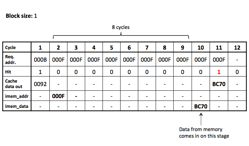
The above two interfaces operate largely independently. The processor is expected to continue to access the cache each cycle until it eventually sees a cache hit. In the background, if a miss occurs the cache sends the request to the memory (assuming it isn't already handling another cache miss). After the correct number of cycles, the cache will then: (1) write the data into the data array and (2) set the tag. The next cycle the processor will then see a cache hit, allowing it to proceed.
In addition to the tag and data, the cache should have a valid bit for each block, which starts with the initial value of "not valid".
Instruction Cache Module Specification
The interface for the Verilog cache module is lc4_insn_cache.v:
`timescale 1ns / 1ps

module lc4_insn_cache (
    // global wires
    input         clk,
    input         gwe,
    input         rst,
    // wires to access instruction memory
    input [15:0]  mem_idata,
    output [15:0] mem_iaddr,
    // interface for lc4_processor
    input [15:0]  addr,
    output        valid,
    output [15:0] data
    );

   /*** YOUR CODE HERE ***/

endmodule
Part C1: Direct Mapped Cache
The initial implementation of the cache is direct mapped, has a block size of a single 16-bit word, and has a total capacity of 256 bytes (27 16-bit blocks).
Part C2: Set-Associative Instruction Cache
Next, implement a two-way set-associative instruction cache by modifying your direct-mapped design. The total cache capacity remains the same as in the previous parts of this assignment.
The cache should implement the LRU (least recently used) replacement policy. Recall that there in a two-way set-associative cache, there is a single LRU bit for each "set" in the cache (and each set has two "ways"). Don't forget the LRU bit is updated on all cache accesses (not just on misses).
Part C3: Four-Word Block Size Cache
The final part of this lab is to extend the cache to have use larger blocks. Instead of a single 16-bit block, modify the cache to use blocks with four 16-bit words. The cache is still two-way set-associative and the total cache size remains the same.
Although the block size is larger, the instruction memory can still supply only a single 16-bit word per cycle. Thus, it will take multiple accesses (and multiple cycles) to fill in the entire cache block. Instead of waiting the entire memory latency before initiating the request for the next word in the block, the interface to memory is pipelined. That is, a new address can be provided to the instruction memory each cycle and the value at the location will be suppled N cycles later.
Below is a cycle diagram for a cache with block size of four. At cycle 2 the instruction requests address 0006. With a block size of four, this address is within the block containing addresses: 0004, 0005, 0006, and 0007. On the same cycle the miss is first detected (cycle 2), the cache requests the first word in the block (0004) from memory. The next cycle (cycle 3), the cache requests the second word (0005) from memory, and so on for the remaining words. The memory returns the four requested words on cycles 10, 11, 12, and 13, respectively. The cycle in which the final word is written into the cache (cycle 13), the cache sets the tag and valid bit. Thus, on the next cycle (cycle 14) the access to 0006 hits in the cache.
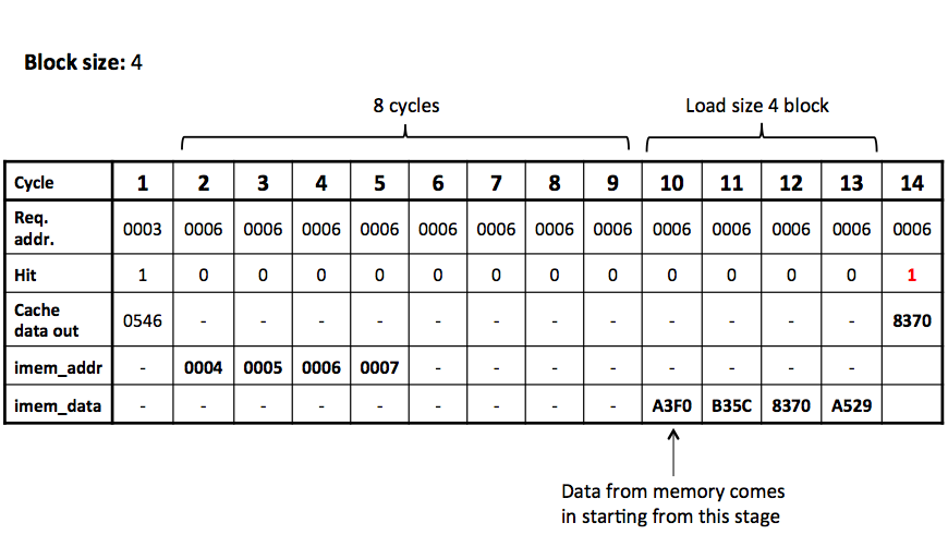
There is one subtle case to consider for multi-word blocks. Prior to filling in the words, the cache should set the block to invalid. This prevents the partially filled block from being accidentally accessed. How could this happen? There is a subtle interaction with pipelining and branch prediction that could trigger the problem. Normally the processor will continue to query the same address over and over again until a hit occurs (as illustrated in the above diagram). However, there is no requirement that the processor must do this. That is, the processor could decide to fetch a different instruction the next cycle instead, for example, due to the resolution of a branch misprediction.
Testing the Cache Module
As we did for the ALU previously, we have provided infrastructure to help you test your code. Verifying that the cache is working correctly requires both "functionality" testing (does it calculate the right answer?) and "performance" testing (does your cache miss the correct amount?). To facilitate both of these, we have provided a stand-alone test fixture, test_lc4_insn_cache.tf, to test your cache implementation prior to integrating it with the processor. This tester checks both the functional correctness and the timing correctness by ensuring that the correct value is returned and the stalls match the expected stalls.
The different cache configurations have different behavior (direct mapped vs set-associative vs multi-word blocks), so we have provided a different input trace for each of these configurations. These various input files can be found in the test_lc4_insn_cache_inputs directory within labfiles.tar.gz. Each file has a name of the form: X_Y_Z.input, in which X is the number of index bits, Y is the number of block offset bits, and Z is the associativity. Thus the configurations that match the above parts are:
- 7_0_1.input - direct-mapped cache with 27 one-word blocks (27 * 16-bits = 256 bytes)
- 6_0_2.input - two-way set-associative cache with 27 one-word blocks (2 * 26 * 16-bits = 256 bytes)
- 4_2_2.input - two-way set-associative cache with 25 22-word blocks (2 * 24 * (22 * 16-bits) = 256 bytes)
We have also included test files for much smaller caches, which you may consider using as smaller caches configurations may be much easier to debug.
Part D: Adding the Instruction Cache to the Pipeline
The final step in the lab is to integrate the instruction cache module into the processor datapath. If the instruction fetch hits in the instruction cache, the datapath acts as normal. If the instruction misses in the instruction cache, the datapath: (1) executes a "no-operation" that cycle and (2) the PC does not change (that is, it will fetch from the same PC the next cycle).
Configuring the Memory
Before integrating the instruction cache, you must configure the instruction memory to have the extra delay cycles the cache module above expects. The files are designed to work both with and without the instruction cache, so to enable the logic such that accessing the instruction memory has non-zero latency, you must change the single line in lc4_memory.v from:
`define INSN_CACHE 0 // False
to:
`define INSN_CACHE 1 // True
Part D1: Integrating the Cache
Below is a revised skeleton of the processor interface (based on the single-cycle datapath from the previous lab) that includes the instantiation of the cache module. In fact, adding the instruction cache to the single-cycle datapath from the previous lab requires changing only a few lines of code, so you may wish to do that before adding the cache to your pipelined datapath from above. But ultimately you must integrate the instruction cache module with your pipelined datapath.
For reference, a skeleton datapath with a cache instantiated: lc4_single_cache.v
`timescale 1ns / 1ps

module lc4_processor(clk,
                     rst,
                     gwe,
                     imem_addr,
                     imem_out,
                     dmem_addr,
                     dmem_out,
                     dmem_we,
                     dmem_in,
                     test_stall,
                     test_pc,
                     test_insn,
                     test_regfile_we,
                     test_regfile_reg,
                     test_regfile_in,
                     test_nzp_we,
                     test_nzp_in,
                     test_dmem_we,
                     test_dmem_addr,
                     test_dmem_value,
                     switch_data,
                     seven_segment_data,
                     led_data
                     );

   input         clk;         // main clock
   input         rst;         // global reset
   input         gwe;         // global we for single-step clock

   output [15:0] imem_addr;   // Address to read from instruction memory
   input  [15:0] imem_out;    // Output of instruction memory
   output [15:0] dmem_addr;   // Address to read/write from/to data memory
   input  [15:0] dmem_out;    // Output of data memory
   output        dmem_we;     // Data memory write enable
   output [15:0] dmem_in;     // Value to write to data memory

   output [1:0]  test_stall;       // Testbench: is this is stall cycle? (don't compare the test values)
   output [15:0] test_pc;          // Testbench: program counter
   output [15:0] test_insn;        // Testbench: instruction bits
   output        test_regfile_we;  // Testbench: register file write enable
   output [2:0]  test_regfile_reg; // Testbench: which register to write in the register file
   output [15:0] test_regfile_in;  // Testbench: value to write into the register file
   output        test_nzp_we;      // Testbench: NZP condition codes write enable
   output [2:0]  test_nzp_in;      // Testbench: value to write to NZP bits
   output        test_dmem_we;     // Testbench: data memory write enable
   output [15:0] test_dmem_addr;   // Testbench: address to read/write memory
   output [15:0] test_dmem_value;  // Testbench: value read/writen from/to memory

   input [7:0]   switch_data;
   output [15:0] seven_segment_data;
   output [7:0]  led_data;


   // PC
   wire [15:0]   pc;
   wire [15:0]   next_pc;

   Nbit_reg #(16, 16'h8200) pc_reg (.in(next_pc), .out(pc), .clk(clk), .we(1'b1), .gwe(gwe), .rst(rst));


   // Stall
   wire          insn_valid;		// Stall if valid == 0
   wire [15:0]   insn_cache_out;

   // Instantiate insn cache
   lc4_insn_cache insn_cache (.clk(clk), .gwe(gwe), .rst(rst),
		              .mem_idata(imem_out), .mem_iaddr(imem_addr),
		              .addr(pc), .valid(insn_valid), .data(insn_cache_out));

   /*** YOUR CODE HERE ***/

   assign test_stall = (insn_valid == 1) ? 2'd0 : 2'd1;

   // For in-simulator debugging, you can use code such as the code
   // below to display the value of signals at each clock cycle.

//`define DEBUG
`ifdef DEBUG
   always @(posedge gwe) begin
      $display("%d %h %h %h %d", $time, pc, imem_addr, imem_out, insn_valid);
   end
`endif

   // For on-board debugging, the LEDs and segment-segment display can
   // be configured to display useful information.  The below code
   // assigns the four hex digits of the seven-segment display to either
   // the PC or instruction, based on how the switches are set.

   assign seven_segment_data = (switch_data[6:0] == 7'd0) ? pc :
                               (switch_data[6:0] == 7'd1) ? imem_out :
                               (switch_data[6:0] == 7'd2) ? dmem_addr :
                               (switch_data[6:0] == 7'd3) ? dmem_out :
                               (switch_data[6:0] == 7'd4) ? dmem_in :
                               /*else*/ 16'hDEAD;
   assign led_data = switch_data;

endmodule
Notice also that test_stall is set to one on a cache miss and to zero otherwise. This allows the same tester module to know when the processor is stalling, and thus that it should not advance the trace of instructions. Thus, the same basic processor test fixture code works (although we did modify it from the previous lab, so you'll want to grab the latest version from the labfiles.tar.gz). The test_stall signal also allows the test_lc4_processor.tf test fixture to output the number of stall cycles.
Test the pipeline + instruction cache with all the .hex files you used to test the pipeline.
Part D2: Running on the FPGA Boards
Show wireframe.hex running correctly on the FPGA boards.
Part D3: Validating Performance
Run house.hex and wireframe.hex and record the stall cycles reported. The stall cycles need not match exactly what we expect, but to receive full credit, the stall cycles should not be much higher or lower than expected.
Demos
There will be two demos:
- Preliminary demo: This demo has two parts:
- Part B1. Demonstrate that test_alu.hex works correctly on your pipeline.
- Part C1. Demonstrate that the basic direct-mapped cache module is working with the stand-alone tester.
- Final demo: Demonstrate your fully-working pipeline
with the instruction cache. This demo includes:
- Demonstrating that the pipeline with instruction cache works on the .hex files we've provided, specifically test_all.hex, house.hex, and wireframe.hex.
- Demonstrating that the pipeline + instruction cache runs wireframe.hex on the FPGA board.
- Recording the stall cycle accounting for traces provided by the TAs, which will check for over-stalling and correct instruction cache operation.
All group members should understand the entire design well enough to be able to answer any such questions. As before, all group members should be present at the demos.
Grading
This lab counts for a significant portion of your lab grade for the course. Rather than giving you a binary all-or-nothing trade-off, I am going to refine it a little bit, allowing you to perform a "partial demo" for partial credit even if your entire design is not working.
- Design document (10%)
- Preliminary demo (30%)
- Part B1 (15%)—test_alu working on pipeline
- Part C1 (15%)—direct mapped cache
- Final demo (55%)
- Part B2-B4 (15%)—pipeline working
- Part C2-C3 (15%)—stand-alone cache module working
- Part D1 (10%)—integrated pipeline + cache working
- Part D2 (5%)—working on board
- Part D3 (10%)—depending on accuracy of stall cycles
- Final writeup & completion of group contribution report (5%)
Late Demo Policy
For those groups that find themselves behind, we will allow groups to demo the above milestones late for half of their value. That is, full credit for whatever you can demo on time and then 50% of whatever you demo at a later time. For both the preliminary and final demos, the "late" demo is by the following Wednesday.
What to Turn In
There will be three documents to turn in via Canvas:
- Design Document. As described above in Part A.
- Final Writeup:
- Design update and retrospective. Write a short "design retrospective", focusing on what you learned during the design that you wish you would have known when you began the implementation. Even if you scored well on your initial design document, you'll probably have uncovered a lot of additional information in your final lab writeup. In the end, how did you actually implemented bypassing and stalling? Etc. Basically, describe how your design changed, what parts you left out of the design document, which parts you got wrong, and assess the effectiveness of your approach to testing and debugging your implementation. What are a few things that, in retrospect, you wish you could got a month back in time and tell yourself about this lab? This shouldn't (just) be a narrative of what when wrong; instead, it should be a critic and analysis of your original design.
- Verilog code. As before, your Verilog code should be well-formatted, easy to understand, and include comments where appropriate. Some part of the project grade will be dependent on the style and readability of your Verilog, including formatting, comments, good signal names, and proper use of hierarchy.
- Assessment. Answer the following questions:
- How many hours did it take you to complete this assignment (total for entire group)?
- On a scale of 1 (least) to 5 (most), how difficult each part of
this assignment?
- Part B (pipeline)
- Part C (cache)
- Part D (integration)
- Group Contribution Report: Finally, to encourage equal participation by all group members, each group member must individually submit (via Canvas) a document describing your view of the contribution of each member of your group. For each group member (including yourself), give a percentage that member contributed to the project and describe their role in the project. The sum of the percentages should add up to 100%.
Hints
- Use good signal names and comments. Using well-named signals and well-documented code will help you and your partner understand each other's code. Plus, this code is complicated enough that good structure, good signal names, and comments really will pay off. I really cannot stress this enough.
- Be careful not to bypass a value from a prior instruction that either doesn't write a register or an instruction that has been squashed due to a branch misprediction.
- Similarly, be sure not to falsely stall any instruction whose encoding might match the previous instruction's output register, but does not actually read the register. For example, the JUMP instruction doesn't read any registers, so it shouldn't be stalled just because the bits in its immediate field happen to match the output register of a prior load. Over-stalling is difficult to detect because it is a "performance bug" and not a "correctness bug". That is, you'll get the right answer, but your processor will have a worse CPI than it should.
- The NZP bits are implicit values that have to be bypassed between register writing instructions and conditional branches. Basically, you can think of the NZP bits as an additional register.
- In several places in the design, you'll have instructions that either (1) don't write a register value (for example, stores) or (2) don't read both input registers (for example, loads). You might consider encoding these cases using an explicit "valid" bit for each 3-bit register specifier. Doing so could dramatically simplify your bypass and stall logic.
- You can implement flushing and stalling (NOP insertion) by using a mux to set the instruction bits to all zeros (which is a NOP in LC4). However, you'll still need to record the source of the stall.
- When a pipeline bubble arrives at the Writeback stage, it is difficult to figure out what caused it to set the test_stall signal correctly. Thus, you will need to remember why different pipeline registers are cleared at those latches and then propagate the information forward. Although you can clear the main pipeline registers, you should not clear the pipeline registers that track why the main pipeline registers were cleared.
Addendum for Next Year
- The lab worked fairly well overall. One potential change to consider is that the stand-alone cache tester and traces did not test for the cases in which the instruction fetch address changes in the middle of a miss (say, due to a branch mis-prediction). From the design retrospective documents, it was clear that this was a major struggle for some groups. I actually had one of the TAs generate some new cache tester traces mid-way through the assignment, but we decided not to give them out in the middle, as it might just increase the confusion. The script in SVN has been updated to generate these newer traces but the traces in the SVN do not reflect the new cases. On the other hand, it gave the students the chance to figure it out on their own, which has some merit, too.