Lab 2 - Single-Cycle LC4 Processor
CIS 371 (Spring 2011): Computer Organization and Design
| Instructor: | Prof. Milo Martin |
|---|---|
| Demo Due: | Thursday, March 31st (you must demo it in the KLab by 7pm) |
| Writeup Due: | Friday, April 1st (turn in PDF via Blackboard by 7pm) |
| Instructions: | This lab should be done in groups of two or three. |
This lab is worth 10% of your course grade.
Announcements
- [March 30] Updated the mc.hex file in labfiles.tar.gz. Hopefully this fixes the outstanding issues. Also, the newest PennSim.jar can load .hex files directly, using the "loadhex" command. Just type in "loadhex mc.hex" in the command line, for example.
- [March 27] Added four new input traces to the labfiles.tar.gz: test_alu.hex, test_br.hex, test_mem.hex, test_all.hex.
- [March 27] Clarifications: We're not asking you to implement the privilege bits and any other aspects to the PSR except just the N/Z/P bits.
- [March 23] Corrected the description of the branch unit to take the PC (and not PC+1) as its input.
Instructions
In this lab, you'll complete a single-cycle LC4 processor. We're giving you the data and instruction memories (including all the I/O devices) . You'll use the register file and ALU from the previous lab, create a branch unit, and design other needed components. The end result is a fully functional LC4 processor complete with video output.
Project Files
A skeleton implementation, including Verilog code for the memory and all of the devices (except for the timer), user constraints, and the missile command memory image on which your processor will be tested is included in the compressed tarball labfiles.tar.gz. To extract the tarball, type 'tar -xvfz labfiles.tar.gz' at the eniac command line.
Important
The labfiles.tar.gz archive also contains new versions of the testbenches and more extensive input files for the modules from the previous lab (ALU and the register file). We strongly suggest that you test your design using these newer testbenches.
Branch Unit Module
Branch Unit Specification
The branch unit module will be in the file lc4_branch_unit.v.:
`timescale 1ns / 1ps

module lc4_branch_unit(insn, pc, nzp, rs_data, next_pc);

   input[15:0]   insn, pc, rs_data;
   input [2:0]   nzp;
   output [15:0] next_pc;

   /*** YOUR CODE HERE ***/

endmodule
The module takes as inputs an instruction (16 bits), the program counter (16 bits), the first register output (16 bits), and the value of the NZP bits (3 bits). The output is the next program counter (16 bits). If the instruction is a non-control instruction, the module should just output the program counter incremented by one. Otherwise, it should calculate the correct next PC.
Branch Unit Implementation
Using the same Verilog subset as used in the previous lab, implement the branch unit.
Branch Unit Testing
The testbench for the branch unit is test_lc4_branch_unit.tf and the input trace is test_lc4_branch_unit.input.
Single-Cycle LC4 Processor
Below is a digram of a LC4 single-cycle datapath using the register file, ALU, and branch unit.
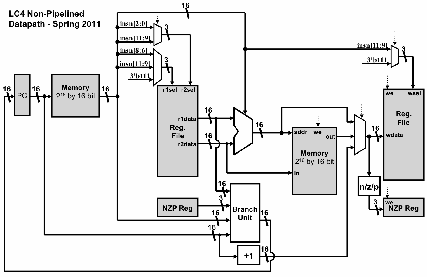
Click on the image for a larger version. It is also available as: lc4_datapath.pdf and lc4_datapath.pptx
LC4 Processor Module
The processor module is in the file lc4_single.v. Most of your code should go into this file, although you want to create and use auxiliary files for sub-modules like the register file, ALU, branch unit, and other modules.:
`timescale 1ns / 1ps

module lc4_processor(clk,
                     rst,
                     gwe,
                     imem_addr,
                     imem_out,
                     dmem_addr,
                     dmem_out,
                     dmem_we,
                     dmem_in,
                     test_stall,
                     test_pc,
                     test_insn,
                     test_regfile_we,
                     test_regfile_reg,
                     test_regfile_in,
                     test_nzp_we,
                     test_nzp_in,
                     test_dmem_we,
                     test_dmem_addr,
                     test_dmem_value,
                     switch_data,
                     seven_segment_data,
                     led_data
                     );

   input         clk;         // main clock
   input         rst;         // global reset
   input         gwe;         // global we for single-step clock

   output [15:0] imem_addr;   // Address to read from instruction memory
   input  [15:0] imem_out;    // Output of instruction memory
   output [15:0] dmem_addr;   // Address to read/write from/to data memory
   input  [15:0] dmem_out;    // Output of data memory
   output        dmem_we;     // Data memory write enable
   output [15:0] dmem_in;     // Value to write to data memory

   output [1:0]  test_stall;       // Testbench: is this is stall cycle? (don't compare the test values)
   output [15:0] test_pc;          // Testbench: program counter
   output [15:0] test_insn;        // Testbench: instruction bits
   output        test_regfile_we;  // Testbench: register file write enable
   output [2:0]  test_regfile_reg; // Testbench: which register to write in the register file
   output [15:0] test_regfile_in;  // Testbench: value to write into the register file
   output        test_nzp_we;      // Testbench: NZP condition codes write enable
   output [2:0]  test_nzp_in;      // Testbench: value to write to NZP bits
   output        test_dmem_we;     // Testbench: data memory write enable
   output [15:0] test_dmem_addr;   // Testbench: address to read/write memory
   output [15:0] test_dmem_value;  // Testbench: value read/writen from/to memory

   input [7:0]   switch_data;
   output [15:0] seven_segment_data;
   output [7:0]  led_data;

   // PC
   wire [15:0]   pc;
   wire [15:0]   next_pc;

   Nbit_reg #(16, 16'h8200) pc_reg (.in(next_pc), .out(pc), .clk(clk), .we(1'b1), .gwe(gwe), .rst(rst));

   /*** YOUR CODE HERE ***/
   assign test_stall = 2'b0; // No stalling to report for single-cycle design

   // For in-simulator debugging, you can use code such as the code
   // below to display the value of signals at each clock cycle.

`ifdef DEBUG
   always @(posedge gwe) begin
      $display("%d %h %b %h", $time, pc, insn, alu_out);
   end
`endif

   // For on-board debugging, the LEDs and segment-segment display can
   // be configured to display useful information.  The below code
   // assigns the four hex digits of the seven-segment display to either
   // the PC or instruction, based on how the switches are set.

   assign seven_segment_data = (switch_data[6:0] == 7'd0) ? pc :
                               (switch_data[6:0] == 7'd1) ? imem_out :
                               (switch_data[6:0] == 7'd2) ? dmem_addr :
                               (switch_data[6:0] == 7'd3) ? dmem_out :
                               (switch_data[6:0] == 7'd4) ? dmem_in :
                               /*else*/ 16'hDEAD;
   assign led_data = switch_data;

endmodule
You will notice that the lc4_processor module has instruction and data memory signals declared in its external interface. The top module is lc4_system.v which instantiates the processor, memory, and devices, and interconnect them to each other and to the pins. In Xilinx, you must set lc4_system.v as the top module or else you will only synthesize the datapath and will not have a full working system.
The lc4_processor module in the lc4_single.v file also has extra outputs that begin with "test" that capture the changes to the processor state after each instruction. Your processor will work even if you don't connect these outputs to anything. As described below, they are provided to help you debug your code both in simulation (so that ModelSim can compare the values you have for these to values in a trace file genrated by PennSim.jar).
Note
What's this "global write enable" or "gwe" all over the place? The block memories in the FPGA are design such that they are read or written on a clock edge. Thus, we don't really have a "single cycle" design. Instead, we use a "global write enable" that is set once every four cycles. This allows reading of an instruction from the instruction memory and then reading/writing from the data memory all in a "single cycle". For the most part this should be transparent to your design.
LC4 Processor Module Implementation
You have the freedom to implement the datapath and control any which way you want. All in all, the processor module should be at most 150-200 lines of Verilog.
Note
One caveat about the dmem_addr bus. This bus should have the value x0000 for any instruction other than a load or a store. The reason is that if this bus accidentally has a value that matches one of the memory-mapped device addresses, you could be unintentionally reading that device.
Note
As was stated in the previous lab, your single-cycle processor will not implement the MOD or DIV instruction. We won't be testing for them explicitly, but it is probably easiest if these instructions just write all zeros into their destination register. Alternatively, you can also implement them as doing nothing.
Debugging Your Processor
Using Trace Simulation
A good way to debug your design is using behavioral simulation and comparison with a trace. The code/ subdirectory in the labfiles/ folder contains several .hex and .trace files. the .hex files are memory dumps of various programs. For example, house.hex is a memory dump of a small non-interactive program that draws the missile command houses on the screen and then exits. house.trace is a trace of that program created by PennSim.
A trace file is a text file containing one line per instruction executed, each with the same fields:
- pc. The PC of the instruction
- insn. The instruction bits themselves
- regfile_we. A bit that indicates if the instruction writes a register
- regfile_reg. The register written by the instruction (if the instruction writes a register)
- regfile_in. The value written to the register file (if the instruction writes a register)
- nzp_we. A bit that indicates if the instruction writes the condition codes (NZP)
- nzp_in. The new NZP bits (if the instruction writes the condition codes)
- dmem_we. A bit that indicates if the instruction writes memory
- dmem_addr. A value of the address accessed by a load or store
- dmem_value. A value that is written to memory (for stores) or read from memory (loads)
The Verilog test fixture test_lc4_processor.tf reads the .trace file, simulates the processor executing the .hex program instruction-by-instruction. When executing, it then compares the lc4_processor module interface signals to the corresponding fields in the trace file, allowing you to debug your implementation instruction by instruction.
The .hex file used to initialize the memory is specified in include/bram.v. Using a different .hex file requires editing the value of the MEMORY_IMAGE_FILE macro at the top of the memory module bram.v. This memory module is used both for simulation and for synthesis, so if you change it in one place it will affect the other.
The labfiles/ contain several tests, which we recommend you use to test your design in the following order:
- test_alu.trace
- test_br.trace
- test_mem.trace
- test_all.trace
- house.trace
The newest versions of PennSim.jar also allows loading of .hex files directly using the new "loadhex" command. Just type in "loadhex mc.hex" in the command line, for example. This will let you single-step through the execution in PennSim during your debugging.
Creating Your Own Tests
The house.hex file was created on PennSim by first loading the object files (ld mcux and ld house) and then using the command: dump -readmemh x0000 xFFFF house.hex. The house.trace file was created on PennSim using the commands trace on house.trace, then break set OS_START, continue and then trace off. You can write your own tests and create your own memory images and trace files in a similar way. You'll need the most recent version of PennSim.jar.
Debugging using Board Single-Stepping
Depending on how you count the processor executes at either 100MHz or 25MHz, but either speed is too fast to debug. You can use the expansion board to put the processor into "single-stepping" mode. Switch 8 controls clock mode: up is "auto", down is "single-step". To step the clock one cycle forward, use the down button on the main board.
When single-stepping through the program, the other expansion board switches determine what value is displayed on the expansion board 7-segment display. What is display is determined by the code at the end of your processor module:
assign seven_segment_data = (switch_data[6:0] == 7'd0) ? pc :
                            (switch_data[6:0] == 7'd1) ? imem_out :
                            (switch_data[6:0] == 7'd2) ? dmem_addr :
                            (switch_data[6:0] == 7'd3) ? dmem_out :
                            (switch_data[6:0] == 7'd4) ? dmem_in :
                            /*else*/ 16'hDEAD;
For instance, when the switches are set to 0 (i.e., all switches down) the 7-segment display shows the value currently on the pc bus, i.e., the program counter. You can also expand this code to get additional debugging info.
Verilog Restrictions
This synthesizable part of this lab should be implemented using the structural and behavioral Verilog subset as in presented in the class notes. The only state element you are allowed to use for synthesis is Nbit_reg. You are allowed to use behavioral Verilog and reg primitives in test fixtures. If you're not sure if you're allowed to use a certain Verilog construct, just ask (post a message on the newsgroup, send an e-mail, etc.).
Demos
During the demo to the TA, you'll demonstrate that your design works using both simulation and the hardware boards:
- Simulation: Using Modelsim, you'll demonstrate that your design works for all the test cases we provided.
- Full Processor Hardware: You'll demonstrate that your design works correctly on your board using the mc.hex and invaders.hex file.
Important
All group members should be present at the demo.
What to Turn In
Turn in a single PDF to BlackBoard that contains all of the following:
- Verilog Code: Your writeup should include Verilog code for the main modules and any sub-modules you created. But not the Verilog code we gave, just the stuff you wrote. Your Verilog code should be well-formatted, easy to understand, and include comments where appropriate (for example, use comments to describe the inputs and outputs to your Verilog modules). Some part of the project grade will be dependent on the style and readability of your Verilog, including formatting, comments, good signal names, and proper use of hierarchy.
- Questions: Answer the following questions:
- Once you had the design working in simulation, did you encounter any problems getting it to run on the FPGA boards? If so, what problems did you encounter?
- What other problems, if any, did you encounter while doing this lab?
- How many hours did it take you to complete this assignment?
- On a scale of 1 (least) to 5 (most), how difficult was this assignment?
- What was the group division of labor on this assignment, in both hours and functional and debugging tasks?